무엇을 찾고 계신가요?
인기 검색어
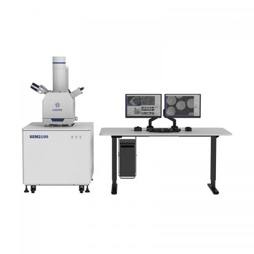
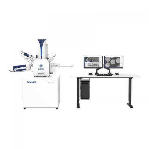
- 전계방출형 주사전자현미경(Field Emission Scanning Electron Microscope) 제조업체 글로벌 공급업체
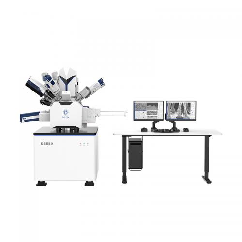
- SEM EDX, EDS, EBSD, BSE, CL, STEM 검출기
- 스캐닝 NV 자력계 양자 다이아몬드 원자현미경 QDAFM 애플리케이션
- ciqtek 스캐닝 NV 센터 현미경 제조업체
- 스캐닝 NV 자기측정 글로벌 공급업체
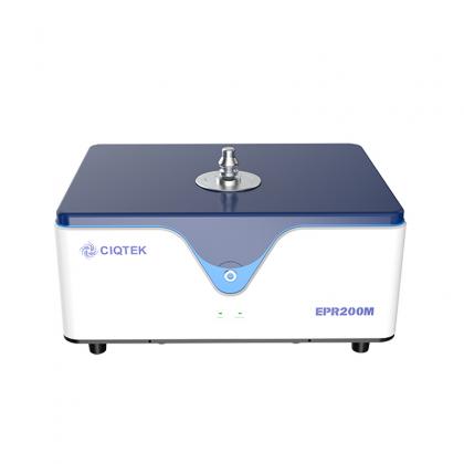
- X-밴드 펄스 전자 상자성 공명 분광학 글로벌 공급업체
- 전자 상자성 공명 분광법 최저 가격
- 저온 유지 장치를 갖춘 X 밴드 EPR 분광학
- W-대역 전자 상자성 공명 분광법 최저 가격
- W-밴드 전자 스핀 공명 분광학 최적 가격